product information
Name: Purple Phosphorus Quantum Dot Dispersion Liquid
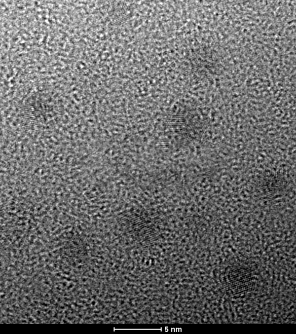
Particle size: 1-10nm
Distribution single layer rate ≥80%
Concentration: ~0.1mg/ml
Packing specification: polar solvents such as water/ethanol/NMP/IPA/DMF/DMSO
Concentration: default 1mg/ml, can be customized
Brief introduction of purple phosphorus product:
In recent years, two-dimensional layered black phosphorus has received extensive attention due to its excellent electrical and optical properties. However, black phosphorus is unstable in water and air, which also limits its applications in the fields of optoelectronics and catalysis.
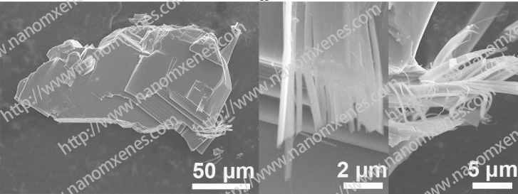
Violet Phosphorus (VP), also as an allotrope of phosphorus, is also a two-dimensional semiconductor material with a layered structure. The three bonds of each phosphorus atom are triangular pyramids, which are stacked to form a tubular chain structure and are arranged in a double layer. , Every two layers are stacked vertically to form a three-dimensional structure, as shown in Figure 1 (monoclinic system, P2/n space group, lattice constant: a = 9.210 Å, b = 9.128 Å, c = 21.893 Å, β = 97.776o). The two layers are connected by van der Waals force, so a few or single layers of purple phosphorus can be obtained by mechanical peeling. Single-layer violet phosphorus is also called violet phosphorene, which is similar to graphene. Theoretical calculations show that violet phosphorene has a high carrier mobility (up to 7000 cm2/Vs, which is equivalent to the theoretical value of black phosphorus), and its band gap has a layer-dependent relationship, from a single layer directly to the band gap (2.54 eV) Indirect band gap (1.7 eV) to bulk material. Theories and calculations show that purple phosphorus is the most stable allotrope of phosphorus and is easily stripped into a single layer.
In short, purple phosphorus combines high carrier mobility and anisotropy, and has the characteristics of wide band gap, stability, and easy peeling. Compared with black phosphorus, purple phosphorus has a broader application prospect in the fields of photonics, electronics and semiconductors.


| Warm tips: Suzhou Beike nano products are only used for scientific research, not for human body,different batches of products have different specifications and performance |
Message
|
|
 |
Scan code concerns WeChat official account
QQCommunication group:1092348845
|
|
| Warm tips: Suzhou Beike nano products are only used for scientific research, not for human body,different batches of products have different specifications and performance.The website pictures are from the Internet. The pictures are for reference only. Please take the real object as the standard. In case of infringement, please contact us to delete them immediately. |